Hello, if you have any need, please feel free to consult us, this is my wechat: wx91due
EEC 210
HW 5
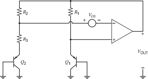
1. The band-gap reference shown below is designed to have nominally zero TCF at 25°C. Due to process variations, the saturation current IS of the transistors is actu- ally twice the nominal value. Assume VOS = 0. What is dVOUT /dT at 25°C? Neglect base currents.
![]()
![]()
![]()
![]()
![]()
![]()
![]()
![]()
![]()
![]()
2. Simulate the band-gap reference from the previous problem on SPICE. Assume that the amplifier is just a voltage-controlled voltage source with an open-loop gain of 10,000 and that the resistor values are independent of temperature. Also assume that IS1 = 1. 25 × 10−17 A and IS2 = 1 × 10⁻¹⁶ A. In SPICE, adjust the closed-loop gain of the amplifier (by choosing suitable resistor values) so that the output TCF is zero at 25°C. What is the resulting target value of VOUT? Now double IS1 and IS2 . Use SPICE to adjust the gain so that VOUT is equal to the target at 25°C. Find the new dVOUT /dT at 25°C with SPICE. Compare this result with the calculations from the previous problem.
3. Calculate the bias current of the circuit shown below as a function of R, µn Cox , and the device sizes. Comment on the temperature behavior of the bias current. For simplicity, assume that Xd = Ld = 0 and ignore the body effect.
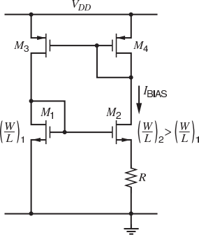
4. The circuit used in the previous problem produces a supply-insensitive current. Calculate the ratio of small-signal variations in IBIAS to small-signal variations in VDD at low frequencies. Ignore the body effect but include finite transistor ro in this calculation.