Hello, if you have any need, please feel free to consult us, this is my wechat: wx91due
EEC 210
HW 7
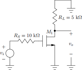
1. a. Use the Miller approximation to calculate the −3-dB frequency of the small-
signal voltage gain of a common-source transistor whose ac schematic is shown below. Assume the dc drain current ID = 0. 5 mA. Also, assume that W = 100 µm, L drawn = 2 µm, Ld = 0. 2 µm, Xd = 0, λ = 0, k′ = 60 µA/V2 , χ = 0, Cdb = 0, Cgb = 0, and fT = 3 GHz (at ID = 0. 5 mA).
b. Calculate the nondominant pole magnitude for the circuit in (a). Compare your answer with a SPICE simulation.
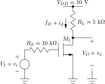
2. For the circuit below, assume that VI is adjusted so that ID = 0. 5 mA. Calculate the low-frequency small-signal voltage gain vo /vi , and use the zero-value time-con- stant method to estimate the −3-dB frequency. Use the same data as in the previous problem except:
a. Cdb ≠ 0. Calculate the zero-bias drain-bulk capacitance as Cdb0 = AD (Cj0′) + PD (Cjsw0′), where AD = (5 µm)W is the drain area and PD = W is the drain perimeter. Let Cj0′ = 0. 4 fF/(µm2 ) and Cjsw0′ = 0. 4 fF/µm. Use Equation (1.202) with ψ0 = 0. 6 V to calculate Cdb . In case you do not have the book, Equation (1.202) shows that 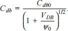
b. Cox ′ = 0. 7 fF/(µm2 ), and fT is no longer given.
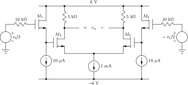
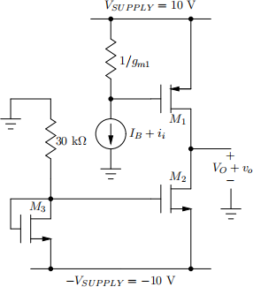
3. Consider the amplifier stage shown below. Assume IB is adjusted so that the dc
output voltage VO = 0.
a. Calculate the low-frequency, small-signal transconductance vo /ii , and use the zero-value time-constant method to estimate the −3-dB frequency. Use the formula for Cdb0 given in Problem 2. For all transistors, assume L drawn = 2 µm, Ld = 0. 2 µm, Xd = 1 µm, χ = 0, W1 = 100 µm, and W2 = W3 = 100 µm. Use Equations (1.201) and (1.202) with ψ0 = 0. 6 V for the junction capacitances. In case you do not have the book, Equation
(1.201) shows that 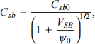 and Equation (1.202) is given in the
previous problem. For M1 , assume Vtp = − 1 V, kp = 20 µA/V2 ,
λp = 1/50 V, Cox′ = 0. 7 fF/(µm2 ), Cj0′ = 0. 2 fF/(µm2 ), and Cjsw0′ = 0. 2 fF/µm. For M2 and M3 , assume Vtn = 1 V, kn = 60 µA/V2 ,
λn = 1/100 V, Cox′ = 0. 7 fF/(µm2 ), Cj0′ = 0. 4 fF/(µm2 ), and Cjsw0′ = 0. 4 fF/µm.
b. Repeat (a) with a 20-pF capacitor connected from the drain to the gate of M1 .
4. An amplifier stage is shown below. Calculate the zero-bias drain-bulk and source-
bulk capacitances as Cdb0 = AD (Cj0′) + PD (Cjsw0′) and
Csb0 = AS (Cj0′) + PS (Cjsw0′), where AD = AS = (5 µm)W is the drain and the source area and PD = PS = W is the drain and the source perimeter. Assume W = 100 µm,Ldrawn = 2 µm, Ld = 0. 2 µm, Xd = 0, λ = 0, k′ = 60 µA/V2 , χ = 0, Vt = 1 V, Cox′ = 0. 7 fF/(µm2 ), Cj0′ = 0. 4 fF/(µm2 ), and Cjsw0′ = 0. 4 fF/µm. Use Equations (1.201) and (1.202) with ψ0 = 0. 6 V for all important junctions. (These equations are given in the previous problems.)
a. Calculate the low-frequency, small-signal voltage gain vo /vi .
b. Apply the zero-value time-constant method to the differential-mode half cir- cuit to calculate the −3-dB frequency of the gain.