Hello, if you have any need, please feel free to consult us, this is my wechat: wx91due
EECS 31L: Introduction to Digital Logic Laboratory (Spring 2025)
Lab 1: Logic Block Design
(Revision: v1.0)
Due: April 13, 2025 (11:59 PM)
In this lab, you will design a few basic logic blocks in Verilog and then verify your designs to see if they work as expected. For each block, you should create a new project, write down the code in Verilog (in *.v source files), and run the simulation in Vivado. Please make sure you complete Lab 0 before working this lab. We use the first block, half adder (HA), as an example to show you the whole process of hardware design and simulation. You should follow the same process for the other blocks. Please read this lab manual carefully and in its entirety.
1 Half Adder (HA)
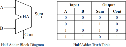
Design a half adder (HA) using Verilog logical operators. As you know, a half adder has 2 1-bit inputs (A and B) and 2 1-bit outputs (Sum and Cout). The block diagram and truth table for a half adder are shown below.
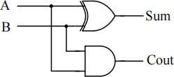
As you see, the Boolean equation for the two outputs (Sum and Cout) are as follow:
• Sum = A XOR B
• Cout = A AND B
And circuit schematic for a half adder is:
Follow these steps to design and simulate a half adder in the Vivado:
• Create a new RTL project in the Vivado.
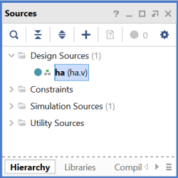
• Add a design source and choose “Create File” (ha.v). Make sure to change the file type to Verilog. You can skip the I/O port definition (you will manually define the I/O ports by commands in your code). Your new source code (*.v) should now be under the “Design Sources” in the “Sources” window.
• Double click on it and enlarge the window. Write the code below and save the file.
Code 1: Half Adder (ha.v).
|
` timescale 1 ns / 1 ps // time - unit = 1 ns , precision = 1 ps ( for simulation // Define the module module ha ( A , B , Sum , C out ); // Define the input and output signals input A ; input B ; output Sum ; output C out ; // Define the modules behavior assign C out = A & B ; // bitwise and assign Sum = A ^ B ; // bitwise xor end module // ha |
• Now to test the functionality of our design, we need to write a testbench. Create a new Simulation Source (ha tb.v) and write the code below.
Code 2: Testbench for Half Adder (ha tb.v).
|
` timescale 1 ns / 1 ps // time - unit = 1 ns , precision = 1 ps ( simulation ) module ha _tb (); // Define the input and output ports reg A_tb = 0; reg B_tb = 0; wire Sum _tb ; wire C out_tb ; // Port Mapping ha instant ( . A ( A_tb ) , . B ( B_tb ) , . Sum ( Sum _tb ) , . C out ( C out_tb ) ); // Test samples initial // initial block executes only once begin A_tb = 1 ' b0 ; B_tb = 1 ' b0 ; # 10; // wait for 10 time - units (10 n s in this example ) A_tb = 1 ' b0 ; B_tb = 1 ' b1 ; # 10; // wait for 10 time - units (10 n s in this example ) end end module // ha _tb |
• Save the code and run the simulation. To simulate the HA tb module, right click on it and click “Set as Top”, then Run the Simulation.
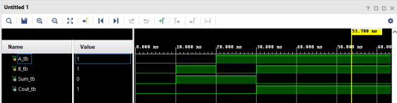
• Check the waveform. From time 0 to 10ns, the inputs are as follows: A=0, B=0, and the outputs are Sum=0 and Cout=0 as expected. For the next 10ns, we have A=0, B=1, and the outputs are Sum=1 and Cout=0. Add a few more tests to the test bench code and see the result on the waveform. Put a screenshot for the waveform for 2 more test cases with explanation in your report.
2 1-bit Full Adder
Now try to design a 1-bit full adder using Verilog logical operators. Below you see the diagram, the truth table, and the circuit schematic for a 1-bit full adder.
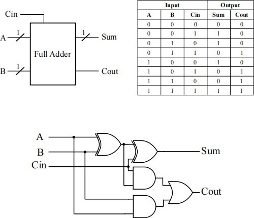
As you see the Boolean equation for the two outputs (Sum and Cout) are as follow:
• Sum = A XOR B XOR Cin
• Cout = (A AND B) OR (A AND Cin) OR (B AND Cin)
Please implement a 1-bit full adder using Verilog logical operators. Define input and output signals and complete the module behavior.
Code 3: 1-bit Full Adder (fa.v).
Simulate your code. Write a test bench for your design and run the tests below.
Test1 (Run for 20ns): A=‘0’ , B = ‘1’, Cin = ‘0’
Test2 (Run for 20ns): A=‘1’ , B = ‘1’, Cin = ‘0’
Test3 (Run for 20ns): A=‘1’ , B = ‘1’, Cin = ‘1’
Put a screenshot of the waveform in your report.
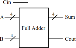
3 4-bit Full Adder
Design a 4-bit full adder in Verilog. Below, you see the block diagram for a 4-bit full adder.
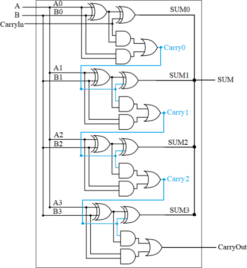
Below is a circuit schematic for a 4-bit full adder. As you can see in the schematic, a 4-bit full adder can be implemented with four instances of 1-bit full adders. Blue lines inside the box are not connected to any input or output ports. We need to define them in the code as wire.
Define signals, complete the code and run the simulation. Write a testbench for your design and run the tests below.
Test1 (Run for 20ns): A=“0110” , B = “0100”, Cin = ‘0’
Test2 (Run for 20ns): A=“1000” , B = “1001”, Cin = ‘1’
Test3 (Run for 20ns): A=“1110” , B = “0010”, Cin = ‘0’
Test4 (Run for 20ns): A=“1010” , B = “1011”, Cin = ‘0’
Check the outputs (Sum and Cout) to see if they are correct. Put a screenshot of the waveform in your report. Your screenshot should show both input and output signals.
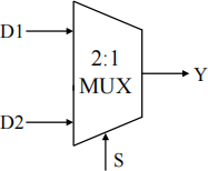
4 2:1 Multiplexer
Design a 1-bit, 2 to 1 multiplexer. You should have a 1-bit select input S that choose from two 1-bit inputs (D1 and D2). When S is ‘0’, the output equals to D1; when S is ‘1’, the output equals to D2. Below is the block diagram for the 2:1 multiplexer.
Use the code skeleton below for your module declaration.
Code 5: 2:1 Multiplexer (mux21.v).
Write a testbench (mux21 tb.v) for your design and run the tests below.
test1 (Run for 20ns): D1=‘0’ , D2 = ‘1’, S = “0”
test2 (Run for 20ns): D1=‘0’ , D2 = ‘1’, S = “1”
Check the output (Y) to see if it is correct. Put a screenshot of the waveform in your report.
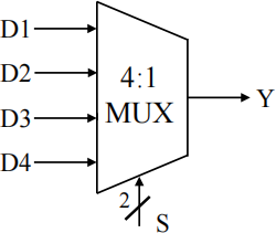
5 4:1 Multiplexer
Design a 1-bit, 4-to-1 multiplexer. You should have a 2-bit select input S to choose from four 1-bit inputs. Below is the block diagram for 4:1 multiplexer.
Use this code skeleton for your design.
Code 6: 4:1 Multiplexer (mux41.v).
Test1 (Run for 20ns): D1=‘0’ , D2 = ‘1’, D3=‘0’ , D4 = ‘1’, S = “00”
Test2 (Run for 20ns): D1=‘0’ , D2 = ‘1’, D3=‘0’ , D4 = ‘1’, S = “01”
Test3 (Run for 20ns): D1=‘0’ , D2 = ‘1’, D3=‘0’ , D4 = ‘1’, S = “10”
Test4 (Run for 20ns): D1=‘0’ , D2 = ‘1’, D3=‘0’ , D4 = ‘1’, S = “11”
Check the output (Y) to see if it is correct. Put a screenshot of the waveform in your report.
6 Assignment Deliverables
Your submission should be in a *.zip file and should be submitted to Gradescope. The ZIP file should include the following items:
• Source Code: Module designs and testbenches. (fa.v, fa tb.v, fa4.v, fa4 tb.v, mux21.v, mux21 tb.v, mux41.v, mux41 tb.v) (Remember: In Verilog the file name does NOT have to be the same as the module name.)
• PDF Report: A report in the PDF format including the simulation results.
Note 1: Start working on the lab as early as possible.
Note 2: Compress all files (8 *.v files + report) into one ZIP file named “lab1 UCInetID firstname lastname.zip”
(note: UCInetID is your email user name and it is alphanumeric string), e.g., “lab1 sitaoh sitao huang.zip”, and upload this ZIP file to GradeScope before deadline.
Note 3: Use the code skeletons given in the lab description. The module part of your code (module name, module declaration, port names, and port declaration) should not be changed.
Note 4: It is fine to discuss the lab with others, but please write the code by yourself.
Note 5: Make sure that your code has good readability, with proper variable naming and comments. You may lose points if your code lacks readability.