School of Computing: assessment brief
|
Module title |
Computer Processors |
|
Module code |
COMP1212 |
|
Assignment title |
Assignment 1: From Truth Tables to Circuits |
|
Assignment type and description
|
In-course assessment. In-course assessment Requires minimisation of Boolean expressions and implementa- tion and testing of circuits in HDL. |
|
Rationale
|
Provides an opportunity to practice tools used to design, implement and test logic circuits to build component parts of computer systems. |
|
Word limit and guidance |
This coursework should take less than 10 hours to com- plete. |
|
Weighting |
40% |
|
Submission dead- line |
10am 14/3/24
|
|
Submission method
|
Gradescope
|
|
Feedback provision |
Feedback will be provided through Gradescope |
|
Learning outcomes assessed
|
Describe the basic building blocks of a computer in de- tail and explain how they are composed to construct computing machinery. Apply appropriate tools to develop, simulate and test logic circuits (CAD). |
1. Assignment guidance
2. Assessment tasks
Your task is to design and implement a circuit in hdl which takes two 2-bit numbers (A, B) and (C, D) as input and produces a 3-bit output (E,F, G).
The final circuit has 6 inputs in total (f1 , f0 ,A,B,C, D) and 3 outputs (E,F, G). The function of the circuit is determined by the two inputs f1 and f0 .
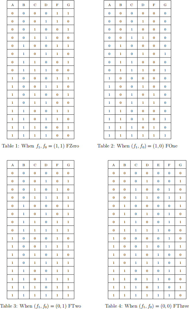
The truth tables below define the operation of the circuit for each combination of f1 and f0 .

(a) For each of the truth tables above, implement a minimal logic circuit in HDL that will perform the function specified by the truth table. You should create one circuit for each truth table and test it produces the required output for that truth table. The circuit for each truth table should be named FZero, FOne, FTwo, FThree corresponding to the names of the truth tables given above and must have corresponding filenames FZero.hdl, FOne.hdl, FTwo.hdl, FThree.hdl. Each circuit must have four inputs named A,B,C and D. Chips FZero, FOne and FTwo will have two outputs (F,G). Chip FThree will have three outputs named E,F and G.
You must only use the built-in AND, NAND, OR, NOR, NOT, Mux, XOR or DMux chips.
The test files provided (.tst and .cmp) can be used to test each output of a chip. For example FZero1.tst tests the F output of the chip FZero.hdl and FZero2.tst tests the G output of FZero.hdl. [9 marks]
(b) Combine all four circuits into one circuit which takes all six inputs and three outputs and test it to ensure it produces the correct output depending on the value of the inputs f1 and f0. Call the chip FALL. You can test this chip using FALL.tst but may wish to create further tests before submission. The value of output is undefined (can be either 0 or 1) unless (f1 , f0 ) = (0, 0)
You must only use the built-in AND, NAND, OR, NOR, NOT, Mux, XOR or DMux chips. [5 marks]
(c) Stretch Activity
When performing computational operations it is often useful to be able to exe- cute a sequence of operations, each one using the output of the previous step as an input to the next step. For example to OR 3 values X OR Y ORZ you might first calculate X OR Y and then on the next step apply ORZ to the previous output (X OR Y).
For this task adapt the circuit FALL so that it can combine a sequence of operations defined by different values for f1 and f0 at each step, by enabling the outputs Ft and Gt of step t to be used (feedback) as the inputs for the next operation Ct+1 and Dt+1 for step t + 1. You should also add a further input (Load) to the chip which when Load = 1 will enable you to load new inputs to Ct and Dt and when set to 0 sets Ct+1 = Ft and Dt+1 = Gt. The Load input will allow you to manually set the values of C and D at the start and during the sequence if required.
Call this chip FSEQ. You can test this chip using FSEQ.tst but may wish to create further tests before submission.
You must only use the built-in AND, NAND, OR, NOR, NOT, Mux, DMux, XOR or DFF chips. [8 marks]
(d) State the function performed by chip FThree. [1 mark]
(e) Explain what function the FALL chip performs and which component of a com- puter system its function is similar to. [2 marks]
(f) Explain what function the chip FSEQ performs. [2 marks]
(g) State the sequence of instructions that would be required to perform the follow- ing operation NOT(4OR2). [2 marks]
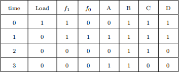
(h) State the single mathematical operation the following sequence of inputs will perform using FSEQ.

[1 mark]
[Total 30 marks]
3. General guidance and study support
Tools required to simulate the hardware and CPU are provided on Minerva under Learning resources: Software.
Please ensure the files you upload work with the test files provided and use the filenames provided in this sheet. Do not alter the format of the lines of these test files in any way. The spacing in each line needs to be preserved You are of course welcome to build your own test files in the same format or add to these files.
Ensure the files you upload pass the submission tests provided on Gradescope. These are not necessarily the same tests as those that will be used to grade your submission.
4. Assessment criteria and marking process
This coursework will be marked using Gradescope. Feedback will be provided through Gradescope and example solutions discussed in class.
Marks are awarded for passing the automated tests on the submitted programs de- tailed below and for answers to the short answer questions
5. Presentation and referencing
Submitted code should provide suitable comments where possible.
6. Submission requirements
Links to submit your work can be found on Minerva under Assessment and feed- back/Submit my work.
For parts (a), (b) and (c) submit only your hdl files, uploaded individually. Ensure you use only the filenames provided in this specification sheet. The names must match the specification exactly, including the use of upper and lower case characters i.e. FZero.hdl is valid however, fzero.hdl or FZero.HDL are not valid.
Parts (d) to (h) should be answered on Gradescope.
7. Academic misconduct and plagiarism
Academic integrity means engaging in good academic practice. This involves essential academic skills, such as keeping track of where you find ideas and information and referencing these accurately in your work.
By submitting this assignment you are confirming that the work is a true expression of your own work and ideas and that you have given credit to others where their work has contributed to yours.
8. Assessment/marking criteria grid
No marks will be awarded for tests which fail or use of chips other than those listed.
. Part (a) There is one test to check the complete truth table for each output of the chips [9 marks].
. Part (b) There are four tests to check the complete truth table of the FALL chip [4 marks].
1 mark will be awarded for a minimised implementation
. Part (c) will be evaluated by testing it on three sequences of functions of various lengths [7 marks].
1 mark will be awarded for a minimised implementation
. Parts (d) to (h) Maximum marks awarded for each question are specified after each part. [8 marks]
[Total 30 marks]