Hello, if you have any need, please feel free to consult us, this is my wechat: wx91due
ECE3020 Final Design Report Guidelines.
1.Perform a design report comparing a MOS inverting amplifier in Figure 1 to one where a BJT substitutes for the MOSFET. Note that the BJT inverter should have some resistance (even 1 ohm) connected to the base. Setup behavioral tests of similar DC sweep, AC sweep, and transient analysis for both inverters. Compare and contrast the 3 behaviors among the 2 inverters. For the MOS case, this is known as a common source amplifier, while for the BJT, this is a common emitter amplifier.
In analog design,transient analysis is typically used to verify AC sweep analysis. In this case, a transient sinusoid is used, at a frequency in the AC sweep passband. Note transient sinusoid needs an offset voltage equal to the operating point Vinq, a small amplitude to maintain linearity. In the transient setup, a stop type is chosen to be long enough to see multiple periods and maybe transient settling. The step time is around 1/5000 of the stop time or less, and in some cases the step ceiling needs to be set with the step value also.
2. Add negative feedback to one of the inverters. CompareDC, AC, and transient behavior with and without feedback.
3. Add an inductor in parallel with the load resistor for either the BJT common emitter or the Vswitch amplifier and analyze the new AC sweep frequency response and transient response (sinusoid in). Use parametric step for 2 values of the load resistor. Comment on the change in gain-bandwidth in the AC response and delay-bandwidth in the transient response.
4. Discuss the MOS differential pair amplifier circuit in Figure 2, as shown on the last page. The differential pair has the flexibility of shifting the “forbidden zone” of the basic inverter. Some MOS op amps are designed using two gain stages, a differential pair amplifier followed by a basic inverter.
The report should have the following sections:
Abstract – write this last, it’s the main things the reader wants to know.
Short problem statement and its answers.
Introduction – Problem context, requirements, and setup.
Results and Discussion – All the technical details.
Conclusion – Review your main results.
The main section is Results and Discussion. This section contains your detailed technical content, such as simulation setups, plots, tables, hand calculations, and your explanations of your technical content. For example, every plot or figure should have some sentences which direct the reader to the main point of the plot or figure.
Analysis tips.
To find gm for MOS you use the same formulas as before, gm = 2*Ib/Vov . For a BJT,
use gm = Ib/25mV (thermal voltage).
Ib is the bias current, a designer usually chooses a desired Ib. For a BJT, Ib sets gm. For MOS, more is needed: Vov = VGS – Vt, where VGS is the dc value. (Vov is the voltage over Vt, same as Veffective). To find Vov, one can set Ib =
(1/2)*kp*(W/L)*(Vov)^2 and solve for Vov. However, a designer usually choose Vov to be small ~200mV. Thus, the designer actually calculates the needed W/L for the transistor. Note that W/L turns out on the order of 100, and you can set kp in thenmos model (the TopSpice default is kp = 20uA/V^2).
The remaining notes (optional) are for the differential pair in Figure 2 (as in an op amp) analysis. The differential pair behaves very much like a common source amplifier.
This is discussed in textbook (Section called: Small-Signal Operation of the MOS Differential Pair) if you want more detail.
From amore simple approach, the 3dB frequency is the same result we’ve seen in a common source amp (low pass filter), equal to 1/RC.
For the AC gain at low frequencies, the gain is equal to gm*R/2. The ½ factor is because Vin is divided evenly in half by the two matched transistors in the differential pair. This is explained in ece5021.
As long as the DC voltage to both input transistors are the same, each transistor will have ½ of the total bias current, eg. 40uA = 0.5*80uA. This is the main advantage of this circuit, the DC input voltage can be adjusted and the bias is independent of Vt.
Finally, keep in mind this circuit is just the main part of an op amp. A better op amp is shown in figure 7.40 and 9.1 (in SedraSmith 5th. ed. Summary Slides), where the input transistors are pMOS instead of nMOS. pMOS inputs are often used, that’swhy we studied the pMOS common source amp. Figure 9.1 shows a second amplifier stage after the diff. Pair. The second stage can have again of about 20, so it’s input doesn’t need to vary by more than 0.25v (for 5v supply). That means the differential pair output doesn’t need to vary by more than 0.25v, so it’s not a problem that the outputs you see in the DC sweep have a limited useful range of 1-2volts at different Vb settings. It’s more than enough.
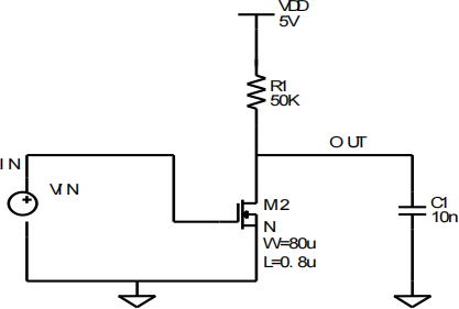
Fig. 1. Common source inverting amplifier.
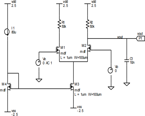
Figure 2. Differential pair amplifier