School of Electronic and Electrical Engineering
ELEC5333M01
Wireless Communications Systems Design
Semester One 2023/2024
ADS Design Assignment
Assignment Information:
. There are 7 pages and four questions to this assignment.
. The question has a recommended page limit. This is to help you determine how long your answer should be. If you submit more than the recommended pages, the additional pages will not be marked.
. All questions should be answered using no more than FIVE A4 pages.
. You should use a minimum font size of 11 point.
. Your work must be typed and machine-readable, not handwritten. Images of hand- drawn diagrams or figures may be inserted into your answer.
. All symbols not specifically defined have their normally accepted meanings.
Academic Integrity:
. You are undertaking this assessment individually and you are expected work independently.
. If you are in any doubt about the University’s expectations for academic integrity, you should review these on the University website:Cheating and plagiarism.
. You should also be aware of the University’s policy on Proof reading.
. Evidence of collusion, similarities between different students' work, copying text, images, or any other content from another source without proper acknowledgement, etc, will be fully investigated.
. You should remember that including an edited version of work obtained from another source is still considered to be a form of plagiarism.
. Please be aware that every submission is automatically checked for similarity to every other submission, internet resources and a repository of all previously submitted work.
Submission instructions:
. You must submit your assignment no later than the submission deadline of before 16:00, UK time, Friday 8th December 2023.
. Your work should be submitted using the Turnitin link within the School Organisation on Minerva.
. You should receive an e-mail receipt from the Turnitin system to confirm that your work has been properly submitted.
. Contact the School if you encounter any difficulties submitting your assignment on Turnitin.
Maximal length of the answer for this question is FIVE pages.
There are various types of antennas that are used in wireless communication. When a group of antennas are placed together the system is called an Antenna Array. Elements in an antenna array are placed in a specific way so that the signals transmitted by each individual antenna sums up so that the overall antenna array can provide better gain, directivity and performance over using a single antenna.
Phased Array Antennas, shown in Fig. 1, as the name suggests, can be termed as an antenna array. What makes them unique is their ability to change the shape and direction of the radiation pattern without physically moving the antennas. This is achieved by transmitting signals of equal frequency from all the individual elements in the array but with a certain phase difference/shift between them. This phase shift will introduce interference between the signals transmitted. The phase shift between the signals should be such that there is constructive interference in the desired direction while destructive interference should occur in other directions.
The interference can be either constructive or destructive, depending on the direction and phase shift introduced between the transmitted signals. In phased array antennas, the phase shift between the signals should be such there is constructive interference in the desired direction while destructive interference should occur in other directions.
Determining the phase shift in accordance with the desired direction of beamforming involves complex mathematical calculations and is done by a computer system.
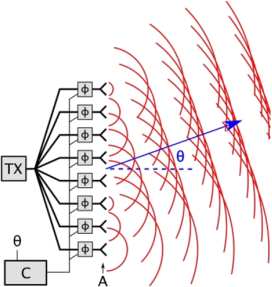
Fig. 1: Basic phased array antennas.
The signal from the transmitter is sent to the antennas via a phase shifter, which is controlled by a computer system (phase controller), that changes the phase electronically thus controlling the direction of the radiation pattern of the antenna array.
Phased Array Antennas consist of multiple smaller antennas whose number can range anywhere from a few antennas to somewhere in the hundreds or thousands.
To reduce the overall size, phased array is best to use phased arrays for higher frequency applications as the antenna size is inversely proportional to the operating frequency so the higher the frequency the smaller the antennas. This makes phased array antennas a great choice for mm-Wave 5G Applications and other high frequency applications as shown in Fig. 2.
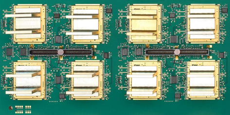
Fig. 2: Phased Array Antennas on a PCB
For a fixed-beam antenna array, the antenna front ends are generally composed of two sections: 1) an antenna array, and 2) power splitter/combiner network.
Microstrip patch antennas
A microstrip antenna in its simplest configuration consists of a radiating patch on one side of a dielectric substrate, which has a ground plane on the other side. The patch conductors usually made of copper or gold can be virtually assumed to be of any shape. However, conventional shapes are normally used to simplify analysis and performance prediction. The radiating elements and the feed lines are usually photo etched on the dielectric substrate. The basic configuration of a microstrip patch antenna is shown in Figure 3.

Fig. 3: Basic configuration of microstrip antenna
The radiating patch may be square, rectangular, circular elliptical or any other configuration. Square, rectangular, and circular shapes are the most common because of ease of analysis and fabrication.
Some of the advantages of the microstrip antennas compared to conventional microwave antennas are:
- Low weight, low volume
- Low fabrication cost,
- Easy mass production,
- Linear and circular polarization are possible with simple feed,
- Easily integrated with MIC,
- Feed lines and matching networks can be fabricated simultaneously with antenna structures.
Patch antennas find various applications stating from military to commercial, because of their ease of design and fabrication. Patch arrays are extensively used in phased array radar applications and in applications requiring high directivity and narrow beamwidth.
As an example, with a given substrate parameters of a substrate with:
Height: 1.6 mm
Metal Thickness: 0.7 mil (1/2 oz. Copper)
Dielectric constant, εr : 4.6
Loss tangent, TanD: 0.001
Conductivity: 5.8E7 S/m
We can calculate the physical parameters of the patch antenna at 2.4GHz as shown in the geometry in Figure 4 using the given formula.
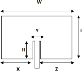
Fig. 4: Geometry of the Square Patch Antenna
The width and length of the radiating surface is given by,

where, velocity of light c = 3 X 10⁸ m/s2, f is the operational frequency and εr is the relative permittivity.
The depth of the feed line into the patch is given by,
H=0.822*L/2 = 12 mm
The other dimensions are,
Y= W/5 = 5.8 mm X = Z = 2W/5 = 11.7 mm
References
- ADS Circuit Design Cookbook 2.0
- A Design Rule for Inset-fed Rectangular Microstrip Patch Antenna
Microstrip Power Divider Design (T-junction power divider)
A power divider is a three-port microwave device that is used for power division or power combining. In an ideal power divider, the power given in port 1 is equally split between the two output ports for power division and vice versa for power combining as shown in Figure 5. Power divider finds applications in coherent power splitting of local oscillator power, antenna feedback network of phased array radars, external levelling and radio measurements, power combining of multiple input signals and power combining of high-power amplifiers.
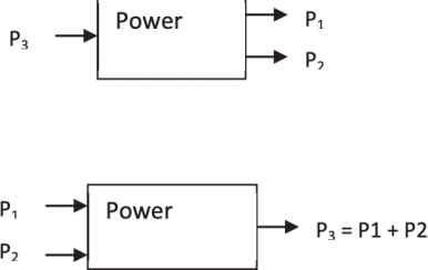
Fig. 5: Model of an Ideal power divider and power combiner
The different types of power divider are T junction power divider, Resistive divider and Wilkinson power and hybrid couplers. The T –junction power divider is a simple 3-port network and can be implemented in any kind of transmission medium like microstrip, stripline, coplanar wave guide etc. Since any 3-port network cannot be lossless, reciprocal, and matched at all the ports, the T junction power divider being lossless and reciprocal and cannot be perfectly matched at all the ports. The T junction power divider can be modelled as a junction of three transmission lines as shown in Figure 6.

Fig. 6: Model of the T- junction power divider and its microstrip layout
To design the T-junction power divider at 3 GHz:
1. Select an appropriate substrate of thickness (h) and dielectric constant (εr) for the design of the power divider.
2. Calculate the wavelength λg from the given frequency specifications as follows:

where c is the velocity of light in air, f is the frequency of operation of the coupler, εr is the dielectric constant of the substrate.
3. Synthesize the physical parameters (length & width) for the λ/4 lines with impedances of Z0 and sqrt2*Z0 (Z0 is the characteristic impedance of microstrip line which is = 50Ω)
References
- ADS Circuit Design Cookbook 2.0
- Microwave Engineering, David M Pozar (downloadable via University of Leeds library):
https://leeds.primo.exlibrisgroup.com/discovery/fulldisplay?docid=cdi_proquest_ebookcentra l_EBC2064708&context=PC&vid=44LEE_INST:VU1&lang=en&search_scope=My_Inst_C I_not_ebsco&adaptor=Primo%20Central&tab=AlmostEverything&query=creator,contains,p ozar
Assignments:
1. Design a single patch antenna at 2.4GHz based on the structure in Fig. 4 with the substrate parameter as follows:
Height: 1.6 mm
Metal Thickness: 0.7 mil (1/2 oz. Copper)
Dielectric constant, εr : 4.6
Loss tangent, TanD: 0.001
Conductivity: 5.8E7 S/m
Show step-by-step calculations and calculated geometries of the rectangular patch antenna [5 marks]. Then, simulate the rectangular patch antenna structure with the calculated geometries using ADS, showing the schematic diagram [5 marks], layout of the antenna [5 marks],simulated S-parameters (return loss) of the single patch antenna [5 marks] and show the radiation patterns and basic antenna parameters such as gain, directivity, and radiation efficiency [5 marks].
2. Design a 1x2 linear antenna array, Fig. 7, based on the single rectangular patch antenna design in 1. First, a 3-dB power splitter must be designed with the input port impedance of 50Ω [5 marks]. Each output port impedance of the 3-dB power splitter must be matched to the input impedance of the patch antenna. Use ADS to simulate the calculated geometries of the 3-dB power splitter, showing schematic diagram [5 marks], layout of the power splitter [5 marks] and S-parameters of the 3-dB splitter [5 marks]. Then, use the designed 3-dB power splitter to connect to the patch antennas as shown in Fig. 7 and simulate the antenna array using ADS. Schematic diagram [5 marks], layout of the antenna [5 marks], simulated S-parameters (return loss) of the single patch antenna [5 marks] and show the radiation patterns and basic antenna parameters such as gain, directivity, and radiation efficiency [5 marks] must be shown.
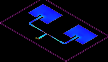
Fig. 7: 1x2 rectangular patch array antenna with 3-dB power splitter T junction feed
3. Design a 2x2 patch antenna array, Fig. 8, based on the single rectangular patch antenna design in 2. Simulate the 2x2 patch antenna array, showing the schematic diagram [5 marks], layout of the antenna [5 marks], simulated S-parameters (return loss) of the single patch antenna [5 marks] and show the radiation patterns and basic antenna parameters such as gain, directivity, and radiation efficiency [5 marks].

Fig. 8: 2x2 rectangular patch array antenna with T junction feed
4. Discuss in detail and compare the technical results of all antenna and T junction power divider designs from 1., 2., and 3. for their performances [15 marks].